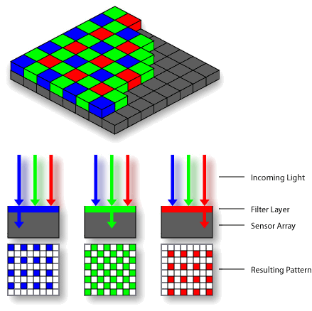
Figure 1 – Schematic of Bayer filter overlain on a CCD (top) also showing how rede, blue, and green light is separated by the filter. From the Wikicommons and in the public domain.
Now that we understand how a charge coupled device or CCD works and how it reads out, we are in a position to consider how exactly one goes about making a color digital camera sensor out of one.The first question is how does one make an intrinsically black and white sensitive sensor sensitive to color. If you followed our discussion about autochromes and additive color, the answer is obvious. You overlay the pixels with some kind of set of red, green, and blue filters. Because everything needs to be electronically addressable and translatable from imaging device to display, say a computer screen, it’s better not to use a random distribution of filters, like in an autochrome, but rather an ordered one. Figure 1 shows schematically such a filter system, referred to as a Bayer filter.
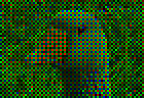
Figure 2 – Image acquired with a CCD chip through a Bayer filter. From the Wikicommons and in the public domain.
Notice that we have twice as many green filters as we do red or blue filters. The reason for this is that the human eye as twice as many green sensitive cells as it does red or blue sensitive ones. Figure 2 shows an example of an image, where we have focussed in very closely so that we can see the individual filters of the Bayer filter. You can do the same thing at home with a digital TV or computer screen and a magnifying glass. So far so good, but there’s a second very important question to consider – the question of how to make the sensor as sensitive as possible. Even though the intrinsic quantum efficiency of a CCD can be remarkably high (as high as almost one electron per photon) several factors conspire against us. There is dead space between pixels and off angle light isn’t going to make it to the photosensitive region.
If you look at Figure 3 you see a schematic of a cross section of a pixel that illustrates several aspects of camera sensor design. Let’s walk through this.
- is the incoming light.
- is a lenslet that collects light to the pixel. It can be shaped so that even light over dead zones makes it to the sensor pixel.
- is the Bayer filter element.
- is the transparent voltage gate.
- is the silicon dioxide insulator.
- is the n-doped silica layer
- is the p/n silica layer
- is the p-doped silica layer.
Figure 3 – Cross section of a pixel on a color digital camera CCD sensor. From the Wikicommons and in the public domain.
The lenslets are very important elements. Without them the device can become quite insensitive. This is especially true as we push greedily for more and more pixels. If you have a certain amount of light striking a pixel and then cut the pixel size in half, so that you have four pixels, where previously there was one, then each pixel gets only a quarter as much light. The well depth similarly goes down. So the bottom line is that you want as much signal as possible. Signal compared to what? Yes you guessed it. Signal compared to noise!
Pingback: Compound vision | Hati and Skoll Gallery