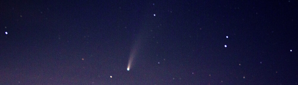
Figure 1 – schematic of the p-n junction of an LED. Top shows distribution of electrons and holes in the two regions. Bottom shows the conductance and valence bands. From the Wikicommons by S-kei and in the public domain under creative common license.
We now have the background information about semiconductors that we need to start to talk about digital photography – about digital array displays and digital sensor arrays. Let’s start with a discussion of LED (light emitting diode) displays. If you sigh at this point and try to escape to elsewhere on the web, chances are that an LED display will still be staring you in the face. If you instead try to escape by watching television, the chances are still very high that an LED display is staring you in the face. So under the assumption that it’s worth knowing as much about your computer as it knows about you, let’s proceed.
In my last technical blog, I discussed p and n type semiconductors. In and of themselves, they’re not too exciting. However, the fun begins when we start to combine them. Suppose we put a p type semiconductor right up against an n type semiconductor. This is what is called a p-n junction. This is also called a diode and is shown graphically in Figure 1, where we’ve even allowed for a small transition region. The p region is shown in blue and the n region in green. You’ll note that we’ve connected this to a battery. The plus terminal to the p side and the negative terminal to the n side, as one might expect. Once the battery is connected, the electrons start to flow towards the plus terminal (remember that opposites attract). Remember also that electrons can flow. Holes really only appear to flow because the electrons are flowing. So there is a current in the semiconductor, with electrons flowing from the n region into the p region and on to the plus terminal of the battery. Of course, electrons exit the negative terminal of the battery and enter the n side of the diode. If you hooked the battery up backwards there would be no current. A diode is unidirectional.
As an aside, in the center we see the symbol for a diode, with its big honking arrow showing the direction that current flows. This is because back in the eighteenth century no less than Benjamin Franklin made the unlucky guess that the charge carrier was not the negative but the positive charge, and this view is perpetrated by convention in circuit theory today, even though everyone knows that it is wrong.
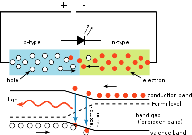
Figure 2 – Large size red, green, and blure LEDs the fundamental components of an LED display. From the Wikicommons by PiccoloNamek and in the public domain under creative common license.
The key thing about the light emitting diode (LED) is that when the electrons enter the p region they recombine with and neutralize holes. This represents as shown in the lower portion of the schematic a transition from the conductance band back to the valence band with the emission of light whose color depends on the transition energy. Hence, electrical energy is converted to light at the junction.
In Figure 2, I show diodes of the three primary colors: red, green, and blue. If you take a magnifying glass up to your LED display, you will see minute arrays of these red, green, and blue LEDs each of which is individually addressable, meaning the light intensity of each can be individually controlled so that whatever color you and intensity you desire is created by additive color. That is basically, how an LED display works.