
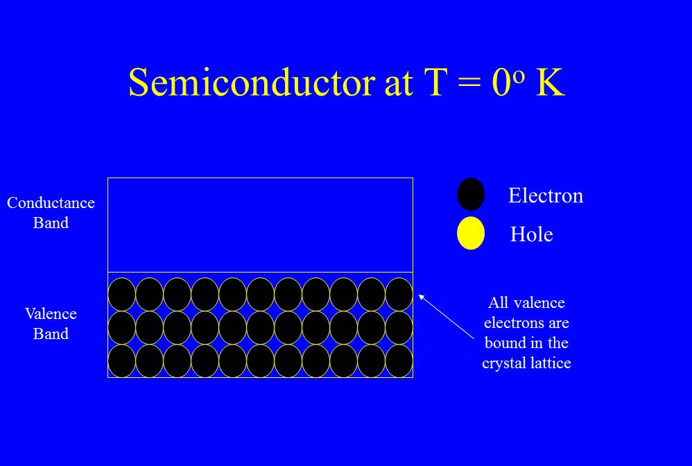
Figure 1 – Schematic of a semiconductor crystal at absolute zero where all of the electrons are bound up by holes. (c) DE Wolf 2013.
As we have seen, the fundamental silver halide chemistry of analogue photography depends upon the physics of semiconductors. And yet, it was developed before anyone knew about semiconductors or even uttered the word. Indeed, in those days they didn’t need to utter the word “analogue” in relation to photography, because there was no digital photography to contrast it with. The same is true for watches. In the “dinosaur ages,” when I was a lad, there were just watches not analogue watches and certainly not digital watches. Indeed, the time is fast approaching when there may be no watches except during retro-fashion fads.
But, as I promised, semiconductors will explain a lot of the technical aspects of digital photography. To get there we need to discuss one more aspect of semiconductor physics – qualitatively I promise.
At absolute zero the valence electrons have no excess kinetic energy and are all sitting in their valence bands. This is shown in Figure 1. All of the positively charged holes are paired up with negatively charged electrons – very boring. Now as we heat up the semiconductor to room temperature, some of the thermal (heat) energy gets absorbed by the electrons and they can escape to the conduction band where they are free to move.
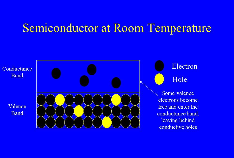
Figure 2 – Schematic of a semiconductor crystal at room temperature where some of the electrons have escaped the lattice and are in the conductance band. There are functionally two types of charge carriers: the free electrons and the positive holes. (c) DE Wolf 2013.
Free to move means that if I attach a battery to two sides of the crystal current will flow. Recognize, that as they flow in the current some electrons may recombine with holes. But then new holes appear as new electrons escape and the net effect is that electrons move form the negative side of the battery to the positive side (remember that opposites attract).
But wait! Imagine that you are watching this process from a distance. Is it the electrons that are moving or is it the holes. They both appear to be moving. It’s like the sensation of being on a train and suddenly the platform appears to be moving. Of course, we know that the electrons have escaped the crystal lattice, while the atoms (holes) have not. But it does look like the holes are moving, and you can even calculate a speed for this motion.
The next question that we need to ask is whether there is a way of modifying the semiconductor crystal so that has more electrons or more holes? Well, remember that whether a material is a conductor, a semiconductor, or an insulators depends on how tightly the valence electrons are bound to the positive atomic nuclei. Remember also that the solid-state crystal acts as a unit not as a set of individual atoms. The net-net of all of this is that if we add a small amount of a material that tends to donate electron the crystal will have more free electrons (in the conductance band). If we add a small amount of a material that tends to bind up electrons (in the valence band) it will have more holes. The materials added are called “doping agents.” Semiconductors with excess negative charge (electrons) are called “n-type semiconductors.” Semiconductors with excess positive charge (holes) are called p-type semiconductors.
The cool thing is that doping can be a very localized process, and as a result, you can build up some very complex semiconductors capable, for instance, of creating a computer and displaying your photographs on a light emitting diode display. That will be the topic of our next technical blog.
Pingback: P-n junctions and the heart of the LED display | Hati and Skoll Gallery