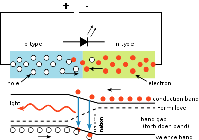
Figure 1 – schematic of the p-n junction of an LED. Top shows distribution of electrons and holes in the two regions. Bottom shows the conductance and valence bands. From the Wikicommons by S-kei and in the public domain under creative common license.