
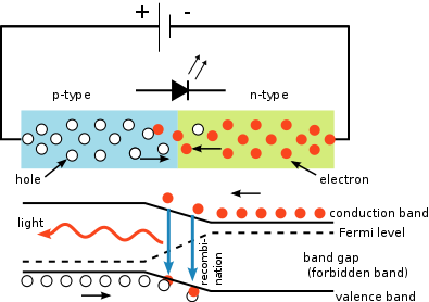
Figure 1 – schematic of the p-n junction of an LED. Top shows distribution of electrons and holes in the two regions. Bottom shows the conductance and valence bands. From the Wikicommons by S-kei and in the public domain under creative common license.
We have previously discussed how a p-n junction can be used to produce a light emitting diode (LED) and how an array of LEDs can be used to create a digital display. I redisplay Figure 1 from that blog to remind you. So lets recall a few critical points. First, the n-type semiconductor is rich in electrons. Second, the p-type semiconductor is deficient in electrons, that is is rich in holes. Second the application of a voltage across the diode (p side positive, n side negative) causes a current to flow and drives electrons from the n-type semiconductor to the junction, where they combine with holes; thus falling out of the conduction band into the valence band. When they do this, they emit light. Hence, we have a light emitting diode.
Now the whole process can, in fact, be reversed. Physicists have a really cool expression. They say that “the system is invariant under reversal of time.” Whoa! Time reversal. Shades of H. G. Wells. Actually this whole question of time reversal in physics is rather fun. In our everyday world time is an arrow. It moves from the past to the present and then on to the future – in inexorably. But the equations of physics they don’t care they can go either way.
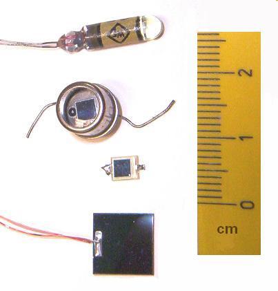
Figure 2 – Examples of discrete photodiode light detectors. From the Wikicommons and in the public domain under GNU licsense
And for our little p-n junction this means that if we can apply a current (aka electricity) and create light we can apply light and get electricity. So if you have a p-n junction and shine light on it (at the correct wavelength), electrons get lifted from the valence band to the conductance band. What happens next depends on whether you have a battery hooked up to it. If you don’t then the electrons build up at the junction creating an electric field or a voltage. The size of the voltage depends upon the amount of light. This is the so-called photovoltaic mode. On the other hand if you attach a battery in the opposite to that shown in Figure 1 (meaning that the plus side is attached to the n-type material and the minus side to the p-type material, referred to as reverse bias) then the as electrons rise to the conductance band they are swept to the positive battery terminal, a current is created.
The reason that the battery needs to be set up reverse bias or backwards to that shown in Figure 1 has to do with our desire to run the system in reverse time. If running electrons one way causes light, we expect that light will cause the electrons to run the other way.
So we can use a p-n junction to create light, a light emitting diode. And we can use a p-n junction to create either a voltage or a current. The latter means that we can use a p-n junction to measure light. Some example of discrete (stand alone) photodiodes are shown in Figure 2. These devices are at the heart (eyes?) of how many light meters on cameras work. And we are one step further to understanding how a digital camera’s detector array works.
Great explanation of esoteric physical phenomena David!